Technology & Services

Expertise in SiC device and package design

SiC Design Services

Cut your time-to-market with NoMIS’ world-leading SiC device and packaging design

Our integrated expertise from device design to packaging and testing, along with proven track record, and global foundry network, helps leading companies develop best-in-class SiC solutions in a fraction of the time.

Our bespoke end-to-end services include:

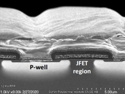
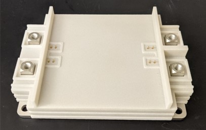
  • Design development for SiC devices (diodes, MOSFETs, JFETs) and modules from 600 V to 13 kV with proven and leading-edge technologies.
  • Testing and qualification support for new designs.
  • Interpretation of analysis and re-engineering to optimize performance.
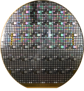
  • Creation and improvement of Process Development Kits (PDKs).
  • Support in establishing the process at a foundry or fab.

Leading-edge IP & know-how

Push the SiC technology frontier with our unique platform of patents, trade secrets, and know-how

With a combined 70+ years experience at the leading edge of SiC technology, NoMIS brings you a unique and expanding portfolio of designs and processes covering:

  • Industry-leading Gen 3 PLANAR MOSFETs and Schottky Diodes.
  • Integrated MOSFETs.
  • Novel next-generation MOSFET designs with enhanced reliability, ruggedness, and lower on resistance.
  • Medium- and high-voltage SiC modules.

Technical Consulting

Develop your SiC Technology Road Map with NoMIS

NoMIS’ team of global SiC experts can help your group navigate a winning path in this critical but complex technology. From helping you understand the current state of the art of SiC and the technology’s future direction to evaluating key investment decisions, we can help you every step of the way.

  • Understand the current SiC market landscape and supply chain.
  • Evaluate the pros and cons of competing technologies.
  • Assess the costs and investment associated with SiC.
  • Develop your own SiC technology road map.
  • Identify sources of talent.
  • Get connected to key supply chain partners.
  • Technical due diligence of vendors, partners, and targets.
  • Train and develop your SiC professionals.

NoMIS SiC Technology

Design and process development, analysis interpretation, and re-engineering to improve foundry PDK and achieve next-generation SiC MOSFET & diode performance

Our design and process recipes have been experimentally verified through 20+ lots at multiple fabrication facilities, ranging from 600 V lateral to 13 kV vertical SiC devices

NoMIS offers fast turnaround of development and prototyping based on prior experience of success and failures, such as custom packaging that takes into consideration both the internal power semiconductor devices, as well as gate driver and converter interfaces

We'll meet your SiC device needs

NoMIS’ unique combination of rare SiC know-how & trade secrets, IP, and global network makes us an ideal partner. Let us help you accelerate your time to market today!

> Learn more

Benefits of working with NoMIS

Reduce your SiC time to market by 3 years or more with our integrated support and proven track record.

Optimize your designs and processes for world-beating performance.

Reach the leading edge of SiC with our next-generation technology.

Access rare world-class SiC talent across device and packaging design and testing.

Tap into our global network of SiC vendors, foundries, and laboratories.